Penn Researchers Take a Big Step Forward in Making Smaller Circuits
Physicists at the University of Pennsylvania have overcome a major hurdle in the race to create nanotube-based electronics. In an article in the August issue of the journal Nature Materials, available online now, the researchers describe their method of using nanotubes tiny tubes entirely composed of carbon atoms -- to create a functional electronic circuit. Their method creates circuits by dipping semiconductor chips into liquid suspensions of carbon nanotubes, rather than growing the nanotubes directly on the circuit.
"Given their amazing electric properties, nanotubes have been a subject of keen interest for creating such things as chemical sensors, flexible electronics and high-speed, high-device-density microprocessors for computing," said Alan T. Johnson, associate professor in Penn's Department of Physics and Astronomy. "The problem is that the properties we like best about nanotubes their size and physical properties also make them very difficult to manipulate."
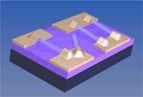
Instead of growing nanotubes in a pattern on a silicon chip, as is conventionally done, the Penn researchers devised a means of "sprinkling" nanotubes onto chips.
"We dip the chips into nanotubes much like dipping an ice cream cone into candy," said Danvers Johnston, a graduate student in Johnson's laboratory and lead author of the study. "Ultimately we can make it so that the nanotubes only stick where want them to in order to form a circuit."
Single-walled nanotubes are formed by turning a single sheet of carbon atoms into a seamless cylinder approximately one nanometer a billionth of a meter in diameter.
Nanotubes can be either semiconducting or "metallic" the latter is highly conductive to electricity depending on the exact geometry of the carbon atoms. Semiconducting nanotubes make for exceptional transistors, which is why so much attention has been devoted to finding a way to use them in electronics.
Previously, most nanotube circuits have been made by growing each nanotube on the surface of a chip, using a process known as chemical vapor deposition. Unfortunately, this method often results in a circuit comprised of both types of nanotubes, metallic and semiconducting. Furthermore, the growth direction of the nanotube is arbitrary, and their diameters are large. Small diameter carbon nanotubes are more useful for switches.
"Fortunately, other researchers have made it possible to grow small diameter nanotubes and to separate metallic from semiconducting nanotubes in solution," said Arjun Yodh, a professor in Penn's Department of Physics and Astronomy. "Ultimately our process can create a large batch of small diameter nanotubes in solution, can separate out the semiconducting nanotubes and then can place them in proper position on a patterned silicon chip."
The researchers, along with post-doctoral associate Mohammed F. Islam, found their biggest challenge in purifying the mass-produced nanotubes. The process they used to create nanotubes in bulk frequently adds impurities usually stray bits of carbon and leftover catalysts that ultimately detract from the quality of the nanotubes.
The Penn researchers found a purification scheme for the nanotubes by heating them in moist air with a gentle acid treatment and then using magnetic fields to separate the nanotubes from the impurities. They deposit the nanotubes by dipping a chip covered with a glue-like substance into the nanotube solution, and then they wash off the excess glue and whatever solvents that remain.
The resulting circuits take advantage of unique electrical properties of nanotubes and can be produced in bulk. Since the researchers can create nanotubes via processes separate from the chips, this process allows for a better control of the quality and diameter. The Penn researchers believe there is a definite role for nanotechnology in the future of electronics.
"The only way to make faster processors is to cram more transistors together," Johnson said. "Nanotubes are just about the smallest transistors that exist right now. So the more densely they can be packed on a chip, the faster the chips can become."
Funding for this research was provided by grants from the National Science Foundation and NASA.
Source: University of Pennsylvania


