Breakthrough in Material Technology: Engineered Nano-Composite Bluestone SL Material for SLA Systems Available

July 29, 2004 Various aerodynamics and Formula 1 prototypes manufactured with Bluestone(TM) SL material from 3D Systems. Images courtesy of Re

3D Systems Corporation announced the availability of Bluestone(TM) SL material, the first commercially available engineered nano-composite resin for SLA(R) (stereolithography) systems.

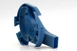
Bluestone(TM) engineered nano-composite material is a breakthrough in material technology, delivering exceptional accuracy, stiffness, thermal performance and long-term stability. Bluestone material is ideal for automotive and aerospace applications, such as wind-tunnel testing, under-the-hood applications, and the manufacture of jigs and fixtures. Its thermal properties are also suitable for elevated temperature electronic applications, including insulating components, electrical housings and connectors.

"Bluestone resin is an excellent fit for applications requiring added stiffness and thermal resistance," said Rainer Neumann, General Manager, 4D Concepts GmbH. "This material is perfect for applications in aerodynamics, lighting applications (such as reflectors), and masters for vacuum casting and thermoforming. As a service provider we need to have flexibility in our material offerings, and Bluestone resin allows us to fulfill many customers' needs for a variety of applications. Now we can offer our customers a unique material with improved part quality and functionality."

Extensive pre-release customer testing has shown the material to facilitate a reliable and predictable build process, to be easy to use and require minimal maintenance.

Stereolithography users will find this material easy to adopt as it requires little or no additional facilities, procedures or expertise, and its performance will extend the range of applications they can address.

Source: 3D Systems


print this article email this article download pdf blog this article bookmark this article     Stumble it Digg this share on Facebook retweet share on Reddit add to delicious
Rate this story - 1 /5 (1 vote)


July 29, 2004 all stories

Comments: 0

1 /5 (1 vote)
  • Stumble this up

  • Digg this

  • share this

  • hide
  • Related Stories

  • Engineers, doctors develop novel material that could help fight arterial disease
    created Nov 25, 2009 | popularity not rated yet | comments 0
  • New hydrogen-storage method discovered
    created Nov 22, 2009 | popularity not rated yet | comments 0
  • Google's Chrome OS to be ready for 2010 holidays (Update)
    created Nov 19, 2009 | popularity not rated yet | comments 0
  • Crashing the size barrier
    created Nov 18, 2009 | popularity not rated yet | comments 0
  • Video fingerprinting offers search solution
    created Nov 09, 2009 | popularity not rated yet | comments 0


Other News

Nanowire Formation

Nanowires key to future transistors, electronics

Nanotechnology / Nanophysics

created 4 hours ago | popularity 5 / 5 (4) | comments 0

(PhysOrg.com) -- A new generation of ultrasmall transistors and more powerful computer chips using tiny structures called semiconducting nanowires are closer to reality after a key discovery by researchers ...


Nanotube defects equal better energy and storage systems

Nanotube defects equal better energy and storage systems

Nanotechnology / Nanomaterials

created Nov 19, 2009 | popularity 4.4 / 5 (10) | comments 2

(PhysOrg.com) -- Most people would like to be able to charge their cell phones and other personal electronics quickly and not too often. A recent discovery made by UC San Diego engineers could lead to carbon ...


Water droplets direct self-assembly process in thin-film materials

Nanotechnology / Nanomaterials

created Nov 23, 2009 | popularity 5 / 5 (4) | comments 2

You can think of it as origami - very high-tech origami. Researchers at the University of Illinois have developed a technique for fabricating three-dimensional, single-crystalline silicon structures from thin films by coupling ...


Using superconducting probes to get a picture of what it's like inside CNTs

Nanotechnology / Nanophysics

created Nov 20, 2009 | popularity 4.4 / 5 (9) | comments 0

(PhysOrg.com) -- "Carbon nanotubes are exciting for fundamental physics, and for potential technological applications," Nadya Mason tells PhysOrg.com. "However, we are generally limited in the way that we can study them. ...


Fast, easy, and highly sensitive arsenic detection with gold nanoparticles

Nanotechnology / Nanomaterials

created Nov 25, 2009 | popularity 5 / 5 (1) | comments 0

(PhysOrg.com) -- Mention of arsenic poisoning usually brings to mind underhanded murder. However, the danger of arsenic poisoning from contaminated drinking water is far greater. Low concentrations of arsenic are found in ...