Researchers develop technique to use dirty silicon, could pave way for cheaper solar energy
A research team led by engineers at the University of California, Berkeley, has developed a new technique to handle metal defects in low-grade silicon, an advance that could dramatically reduce the cost of solar cells.
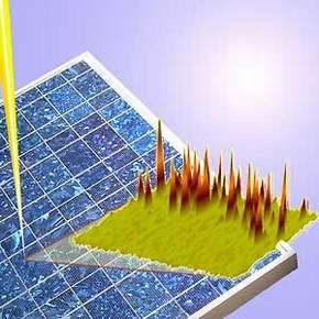
Image: Artist's impression of an intense beam of synchrotron radiation (from the upper left) striking a solar cell, imaging the iron impurity. (Image courtesy Tonio Buonassisi/UC Berkeley)
Nearly 90 percent of solar, or photovoltaic, cells in the world are made from a refined, highly purified form of silicon, the same material used to make integrated circuits. The growth of the semiconductor and solar cell industries has put increasing pressure on relatively limited supplies of this high-quality silicon, consequently driving up the price of the material.
Attempts to use the far more abundant and cheaper form of silicon - one that is laden with metal impurities and defects - have failed because solar cells made from this material do not perform as well. In addition, manufacturing techniques used to remove impurities are expensive, negating the cost benefits of using the cheaper material.
"We have proposed a new approach to the use of dirty silicon," said Eicke Weber, UC Berkeley professor of materials science and engineering, principal investigator of the Center for Advanced Materials at the Lawrence Berkeley National Laboratory (LBNL), and principal investigator of this research project. "Instead of taking the impurities out, we can leave them in but manipulate them in a way that reduces their detrimental impact on the solar cell efficiency."
Other UC Berkeley researchers on the project are Tonio Buonassisi, a Ph.D. student in materials science and engineering, and Andrei Istratov, assistant research engineer, both of whom are also affiliated with LBNL. Also on the team are Matthew Marcus at LBNL's Advanced Light Source, Barry Lai and Zhonghou Cai at Argonne National Laboratory's Advanced Photon Source, and Steven Heald at the Pacific Northwest National Laboratory.
The researchers say the findings, published Aug. 14 in the journal Nature Materials, could dramatically reduce the cost of solar cells by making the use of cheaper materials feasible.
"Solar energy is often touted as the most promising and secure alternative energy source, capable of reducing our dependence on foreign fuels while reducing the emission of dangerous gases that harm world climate," said Weber. "The current worldwide growth rate of photovoltaics is 30 to 45 percent per year, which is nothing short of amazing. However, the solar energy industry could grow much faster if researchers and manufacturers could further reduce the cost of solar cells."
The team analyzed how metal contaminants in silicon respond to different types of processing using highly sensitive synchrotron X-Ray microprobes capable of detecting metal clusters as small as 30 nanometers.
The researchers found that the nano-sized defects scattered throughout the silicon limited the average distance electrons were able to travel before losing their energy. The longer the distance, known as the minority carrier diffusion length, the greater the energy conversion efficiency of the material.
"We found that one way of managing these nano-sized metal defects is to round them up into large groups so that they are less disruptive to the electrons," said Buonassisi. "Compare the metal particles to having hundreds of horses scattered loose on the streets of Berkeley. They would be very disruptive to traffic. But if we corralled the horses together in one pen, people and traffic could move around them more freely."
The researchers found that they were able to manipulate the distribution of the metal impurities by varying the cooling rate of the silicon. When the material is cooled quickly, the metal defects are quickly locked in a scattered distribution. By simply slowing down the cooling rate, the metal impurities diffused into large clusters.
"Using this cooling technique, we were able to improve the distance electrons could travel by a factor of four compared with dirty silicon that had been left unaltered," said Buonassisi. "Although this is still not as efficient as ultrapure silicon, it is the proof of principle that poor-quality silicon can be easily improved. We are now looking at other techniques that could further enhance the efficiency of dirty silicon."
The researchers point out that techniques such as varying the cooling rate of silicon is an easy, cost-effective adjustment to current manufacturing procedures.
"We're targeting mainstream technology," said Weber. "The approach we are proposing could lead to substantial progress in making solar energy more widely available with just a few tweaks in the manufacturing process."
The researchers say that by 2006, the photovoltaic industry is projected to use more silicon than the microelectronic industry, and that keeping solar energy cost-effective may depend upon finding ways to utilize the dirtier, cheaper silicon material.
"As solar electricity moves into mainstream power generation, the production of high-quality silicon has not kept pace with demand," said Istratov of UC Berkeley. "The resulting shortage in supplies of high-grade silicon has caused its price to increase by up to 800 percent on the spot market. Since the solar cell wafer comprises more than half of the cost of the solar cell device, this has translated into recent price increases for solar cells. We believe that our engineering concept has the potential to help the photovoltaic industry remain competitive as an alternative energy source."
The research is supported by the U.S. Department of Energy's National Renewable Energy Laboratory and its University Crystalline Silicon Research Project.
Source: UC Berkeley


