New Microprinting Technique Improves Nanoscale Fabrication
Scientists will announce next month a new technique called microdisplacement printing, which makes possible the highly precise placement of molecules during the fabrication of nanoscale components for electronic and sensing devices.
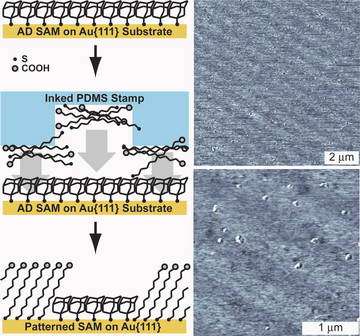
Image: A demonstration of microdisplacement printing, in which a weakly bound film is displaced by contact stamping with molecules that bind more strongly to the substrate. This process leaves a patterned film with regions of strongly bound molecules (where the weakly bound molecules were displaced) and regions of the remaining weakly bound molecules.
(Left) A schematic of the microdisplacement printing process, using a 1-admantanethiolate self-assembled monolayer as the weakly bound film and 11-mercaptoundecanoic acid as the displacing ink molecules on a striped stamp.
(Right) Lateral force microscopy images of a sample made by the microdisplacement printing. The higher friction (shown as light) stripes are the ink. The lower friction (shown as dark) stripes are the remaining, undisplaced 1-adamantanethiolate regions.
The new technique, which also extends the library of molecules that can be used for patterning, will be described in the 14 September issue of the journal Nano Letters by a team led by Paul S. Weiss, professor of chemistry and physics at Penn State.
The new microdisplacement technique is based on a widely used patterning method known as microcontact printing - a simple way of fabricating chemical patterns that does not require clean rooms and other kinds of special and expensive environments. Both methods involve "inking" a patterned rubber-like stamp with a solution of molecules, then applying the inked stamp to a surface.
"Microdisplacement gives us more control over the precision with which the patterns are placed and retained, and also allows us to use a wider range of molecules," Weiss says.
One of the limitations of microcontact printing is that its precision is limited at the edges of a stamped pattern by the tendency of the applied molecules to skitter across the stamped surface, blurring or obliterating the applied pattern and destroying its usefulness.
Weiss's improved microdisplacement technique solves this problem by applying a self-assembled-monolayer film - a single ordered layer of spherical adamantanethiolate molecules - to keep the stamped molecules in place on the surface.
"We specifically engineered the adamantanethiol molecule to have a very weak chemical bond with the surface so that it would detach easily when bumped by a stronger-bonding molecule," Weiss explains.
The molecules inked on the stamp replace the adamantanethiolate molecules wherever they touch the monolayer film, but the surrounding molecules in the film remain attached to the surface to prevent the applied molecules from wandering.
"Microdisplacement printing uses many of the same procedures as microcontact printing except one first prepares the substrate by coating it with a self-assembled monolayer of adamantanethiolate, which is inexpensive and easy to apply," Weiss explains.
"You dip the substrate in a solution of these molecules, pull it out, and they assemble themselves into an ordered film one molecule thick."
In addition to providing more control over the precision of stamped patterns, the new microdisplacement technique also relaxes the requirements in precisely positioning a series of stamps used to apply consecutive patterns with different molecular inks.
"You don't have to be extremely precise about the exact placement of the stamps as long as you apply the molecular inks in order of their bonding strengths," Weiss explains. Each successive layer of molecules either will displace or will not displace the already-applied molecules, depending on their relative bonding strengths with the underlying surface.
The research was aided by the Weiss lab's unusual collection of microscopes, which enable the scientists to get a clear picture of the results of their experiments, both at the broad scale of a stamped pattern and at the narrow scale of just a single molecule.
One scanning tunneling microscope that Weiss and his group designed and built themselves, for example, has 1,000 times more resolution than is needed to image an individual atom.
Adamantanethiol is related to the family of alkanethiol molecules, which have been studied extensively as a model systems for their ability to form well-ordered monolayer films on gold.
Weiss and his team were studying the adamantanethiolate-on-gold system when graduate student Arrelaine Dameron discovered that stronger-bonding molecules easily displaced the adamantanethiolate molecules.
Her discovery has led to further studies of this system by the Weiss team, including how the displacement can be applied in a broad range of applications using a variety of materials.
"We have mapped out strategies in this model system and are now investigating how we can apply these strategies more broadly as the chemistry is developed for self-assembled monolayers on other substrates, especially semiconductors," Weiss says.
"Our goals are to see how far we can take these kinds of simple techniques, along with our knowledge of intermolecular interactions, to bridge the 1-to-100-nanometer length scale in nanofabrication, which even at the high end currently requires very difficult, slow, and expensive techniques."
In addition to Weiss and Dameron, the Penn State research team includes postdoctoral fellows Jennifer Hampton and Susan Gillmor and graduate students Rachel Smith and T. J. Mullen. The research was supported by the Air Force Office of Scientific Research, the Army Research Office, the Defense Advanced Research Projects Agency, the National Science Foundation, the Office of Naval Research, and the Semiconductor Research Corporation. The work was performed as a part of both the Center for Nanoscale Science and the National Nanofabrication Infrastructure Network.
Copyright 2005 by Space Daily, Distributed United Press International


