Study suggests new way of making super-hard nanomaterials
Research conducted by a team of scientists led by Lawrence Livermore National Laboratory suggests a new way of making super-hard materials under high-pressure conditions. The research offers a glimpse at harder materials that could one day be used in fusion energy production, spacecraft shielding and safer automobile frames, as well as other applications.
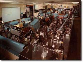
Image: Livermore’s Janus laser was used to generate shock waves in nanocrystalline nickel and copper nearly one million times greater than atmospheric pressure.
The findings, under the title “Ultrahigh Strength in Nanocrystalline Materials Under Shock Loading,” are reported in the Sept. 16 edition of the journal Science.
“This marks the first time anyone has been able to do actual shock experiments on nanocrystal metals and, at the same time, carry out numerical simulations in supercomputers to interpret the results,” said Eduardo M. Bringa, a materials scientist at LLNL and the principal investigator on the team.
Until now, understanding of how nanocrystalline metals deformed at high strain rates had been limited to computer simulations. For their research, Lab scientists introduced shock waves via the Laboratory’s Janus laser.
Their findings point the way to making materials harder than anything previously achieved.
In general, metallic materials used in everyday applications are made of small “grains” joined by grain boundaries. When the grain size is reduced to less than 100 nanometers, the material is considered “nanocrystalline.” (As a reference point, human hair has a thickness of 1-10 microns; 1 micron equals 1,000 nanometers.)
Nanocrystalline materials have extraordinary properties, such as enhanced hardness. However, when the grain size becomes extremely small, the grains slide over each other as the material deforms, causing the material to become softer.
“It’s sort of like stepping into sand,” said Bruce Remington, a laser physicist at the Lab and a participant in the research. “The material is solid but you still sink into it.”

The Lab-led team studied what happened when a shock wave was passed through samples of nanocrystalline nickel and copper. In addition to the experiments, they carried out simulations using up to 4,000 processors in LLNL computers. These are the largest simulations of nanocrystals to date. The shock waves produced by the high-intensity laser move faster than the speed of sound and generate pressures nearly one million times greater than atmospheric pressure.
“This high pressure increases the friction among grains and decreases the sliding,” Bringa said. “By turning off the mechanism that softens the grains, we create a material that, being hard to begin with, is even harder during and following the shock wave application.”
Remington cautioned that the research remains in early phases, but said such research could point the way to harder materials that could be used in shielding military vehicles, protecting spacecraft from damage caused by interplanetary dust particles, or fashioning safer bumpers and automobile frames. The materials also could have applications in inertial confinement fusion experiments.
In addition to Bringa and Remington, LLNL team members include Alfredo Caro, Yinmin (Morris) Wang, Maximo Victoria and James McNaney, of the Materials Science and Technologies Division within the Chemistry and Materials Science Directorate; and Raymond Smith of the Physics and Advanced Technologies Directorate. The Paul Scherrer Institute in Switzerland also contributed.
Bringa said the team has not yet been able to measure what happens during the shock wave transit, which lasts only nanoseconds, “but we have studied how the material changes after shock loading.” As part of this ongoing project, Bringa said the team will continue collaborating with worldwide experts in order “to improve our understanding of the interesting nanocrystalline materials.”
Plans are in place to do the first time-resolved measurements at the Janus laser, to refine the understanding of the shocked nanocrystalline samples.
Source: Lawrence Livermore National Laboratory


