C<sub>60</sub> increases gain in organic-metal-semiconductor transistors

May 4, 2004 C60_resize

I. A. Hümmelgen and group of scientists from Brazil and UK implemented C60 to metal-base transistor technology.
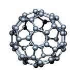
They used evaporated C60 as the emitter in a vertical transistor structure with Au base and Si collector. The proportion of emitted electrons that overcome the barrier is measured as at least 0.99. This metal-base transistor is easy to fabricate as it does not involve wafer bonding or require perfect semiconductor-on-metal growth.
Recent article has been published in Applied Physics Letters (Vol. 84, No. 20, pp. 3978–3980)

All-inorganic metal-base transistors (MBT) with magnetic base have attracted great interest for use as sensors. The spin-valve effect (also called giant magnetoresistance) has led to an intense research activity worldwide, motivated both by the enormous potential for read heads for magnetic recording and the fundamental interest of the physical phenomena. Since its discovery in 1988, magnetic-field sensors based on the giant magnetoresistance of magnetic multilayers have been the subject of much investigation.
Nevertheless, inorganic MBTs have very low current gains, as well as being difficult to fabricate. These problems may be overcome with the use of an organic emitter.

The MBT consists of an ultrathin metal layer (the base), sandwiched between two semiconductors (the emitter and the collector). Like a conventional bipolar transistor, the MBT is a three-terminal device with a forward biased emitter-base junction and a reverse-biased base-collector junction. However, in the MBT these are Schottky junctions rather than p–n junctions.

A straightforward modification to the basic MBT design that authors introduced solves both of the problems present in conventional inorganic MBTs mentioned above, though at the cost of requiring high operating potentials. This improvement is achieved using fullerene C60 as the emitter material. It demonstrates the feasibility of using organic materials as the emitter in hybrid organic–inorganic transistor structures functioning by the injection of a current across an ultrathin base layer.


print this article email this article download pdf blog this article bookmark this article     Stumble it Digg this share on Facebook retweet share on Reddit add to delicious
Rate this story - not rated yet


May 4, 2004 all stories

Comments: 0

not rated yet
  • Stumble this up

  • Digg this

  • share this

  • hide
  • Related Stories

  • Fullerenes and nanotubes are back in the news
    created May 12, 2004 | popularity not rated yet | comments 0
  • Organic Transistors: Researchers produce high performance field-effect transistors with thin films of Carbon 60
    created Nov 26, 2007 | popularity not rated yet | comments 0
  • Bouncing Bucky Balls
    created Oct 16, 2007 | popularity not rated yet | comments 0
  • Selling chip makers on optical computing
    created Nov 24, 2009 | popularity not rated yet | comments 0
  • Battery Research Aims To Store Renewable Energy
    created Nov 19, 2009 | popularity not rated yet | comments 0


Other News

Nanotube defects equal better energy and storage systems

Nanotube defects equal better energy and storage systems

Nanotechnology / Nanomaterials

created Nov 19, 2009 | popularity 4.4 / 5 (10) | comments 2

(PhysOrg.com) -- Most people would like to be able to charge their cell phones and other personal electronics quickly and not too often. A recent discovery made by UC San Diego engineers could lead to carbon ...


Water droplets direct self-assembly process in thin-film materials

Nanotechnology / Nanomaterials

created Nov 23, 2009 | popularity 5 / 5 (4) | comments 2

You can think of it as origami - very high-tech origami. Researchers at the University of Illinois have developed a technique for fabricating three-dimensional, single-crystalline silicon structures from thin films by coupling ...


Fast, easy, and highly sensitive arsenic detection with gold nanoparticles

Nanotechnology / Nanomaterials

created Nov 25, 2009 | popularity 5 / 5 (1) | comments 0

(PhysOrg.com) -- Mention of arsenic poisoning usually brings to mind underhanded murder. However, the danger of arsenic poisoning from contaminated drinking water is far greater. Low concentrations of arsenic are found in ...


Using superconducting probes to get a picture of what it's like inside CNTs

Nanotechnology / Nanophysics

created Nov 20, 2009 | popularity 4.4 / 5 (9) | comments 0

(PhysOrg.com) -- "Carbon nanotubes are exciting for fundamental physics, and for potential technological applications," Nadya Mason tells PhysOrg.com. "However, we are generally limited in the way that we can study them. ...


Peptides control crystal growth with 'switches, throttles and brakes'

Peptides control crystal growth with 'switches, throttles and brakes'

Nanotechnology / Bio & Medicine

created Nov 23, 2009 | popularity 4.8 / 5 (4) | comments 0

(PhysOrg.com) -- By producing some of the highest resolution images of peptides attaching to mineral surfaces, scientists have a deeper understanding how biomolecules manipulate the growth crystals. This research ...