The World’s Smallest Fountain Pen?
The miniscule tip on an atomic-force microscope (AFM) helps researchers both "see" and manipulate the nanoscale environment. Now, engineers have created two novel technologies that enable such tips to write features as small as viruses and to withstand abuse with the resilience of diamond. Eventually, they believe, vast arrays of such nanofountain probes could prove useful for crafting such intricate systems as protein arrays or complex semiconductors.
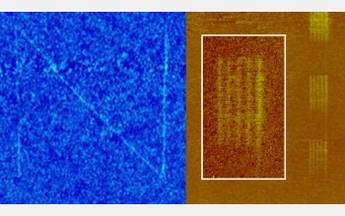
Image: Horacio Espinosa and colleagues at the NSF Nanoscale Science and Engineering Center for Integrated Nanopatterning and Detection Technologies created these two frictional atomic force microscopy images using the new nanofountain probe. The line widths on the letter "N" are as thin as 40 nanometers, and the swatches in the right-side image are less than 10 microns long. The inset on the right-side image shows pattern detail. Credit: © 2005 Horacio D. Espinosa
By taking advantage of the same capillary forces that keep fountain pens flowing, researchers from Northwestern University in Evanston, Ill., created a specialized structure that channels inks from a tiny reservoir down to a miniscule AFM tip.
Existing "dip-pen" techniques utilize the same inks, which range from pigments for creating patterns to organic materials for creating sensors, but they suffer from difficulties with maintaining a regular ink supply. The new "nanofountain probe" can paint features as small as 40 nanometers and carries its own ink reservoir.
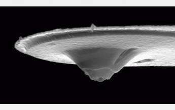
Image: This scanning electron micrograph shows the new nanofountain-probe dispensing tip. Credit: © 2005 Horacio D. Espinosa
Horacio Espinosa and colleagues from the NSF Nanoscale Science and Engineering Center for Integrated Nanopatterning and Detection Technologies crafted the probe using standard microfabrication techniques, so device production is scalable.
The center, a collaboration among researchers from Northwestern University, the University of Chicago, the University of Illinois at Urbana-Champaign and Argonne National Laboratory, was also behind the development of another AFM breakthrough, single-piece, ultra-nano-crystalline diamond cantilevers and tips.
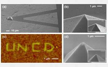
Image: This slide highlights the ultra-nano-crystalline diamond (UNCD) atomic force microscope (AFM)cantilever. (a) This is a scanning-electron micrograph of a UNCD cantilever with a tip. (b) This is a scanning electron micrograph of a UNCD tip after one hour of scanning on a diamond substrate. Inset shows the tip before the scanning. (c) This is a frictional AFM image of an alkanethiol monolayer patterned onto a gold substrate with a UNCD tip. Researchers used the same tip for patterning and imaging. (d) This scanning electron micrograph shows a commercially available silicon nitride tip after one hour of scanning with the same parameters used for the UNCD tip in (b). The image shows damage at the tip apex while the inset shows the tip prior to the test. Credit: © 2005 Horacio D. Espinosa
Existing commercially available tips incorporate a diamond tip glued to a cantilever, a difficult component to craft, or less durable silicon tips coated with layers of diamond.
In addition to being extremely durable, the new tips are also crafted using standard microfabrication techniques and offer the same manufacturing advantages as the nanofountain probes.
Both developments appeared in the journal Small. A report on the nanofountain probe appeared in the April 2005 issue, and one on the ultra-nano-crystalline diamond tip appeared in the August 2005 issue.
The research was supported by NSF.
Source: NSF (by Josh Chamot)


