Samsung Develops 2Gb Flash Memory Using 60nm Process
Samsung Electronics Co., Ltd., the world leader in advanced memory technology, announced today that it has successfully developed a faster and higher capacity version of the world's fastest memory chip.-- OneNAND TM -- while applying 60nm technology to the chip's production process for greater manufacturing efficiency.
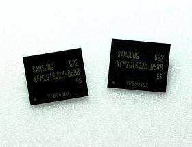
The new 2Gb OneNAND chip doubles the capacity of a OneNAND memory device (from 1Gb) and increases the chip's ‘write' speed from 9.3MByte to 17MByte per second.
”We're seeing a rapidly widening market for our OneNAND memory because of its outstanding performance and capacity that has become even more noteworthy with the application of 60 nm technology,” said Don Barnetson, Director, Flash Marketing, Samsung Semiconductor.
Featuring NOR flash memory's fast ‘read' speed and NAND flash's high-capacity plus fast ‘write' speed, OneNAND holds enormous market potential in a wide range of applications from multimedia phones to digital cameras, removable memory cards, PCs and digital TVs.
Moreover, the chips can be interleaved to attain an even higher capacity, while allowing each chip to independently interact with the system. The more chips that are interconnected the more data that can be processed. For example, the ‘OneNAND chip's write' capacity can be increased up to 136MByte per second when eight of the 2Gb memory chips are combined.
OneNAND memory can be used as buffer memory not only for ‘writes' in the system – by using faster-than-NAND ‘write' speeds, but also as a buffer for high-performing ‘read' operations.
Because of its exceptionally high performance, OneNAND can serve as a catalyst in the development of new product markets. A much-discussed example of this application-creating role is in how OneNAND memory is now being specified as the buffer memory inside a hybrid hard disk.
Samsung successfully demonstrated a commercial Hybrid-HDD prototype for the first time at the MS Developer Conference (WinHEC: Windows Hardware Engineering conference) in Seattle last month.
Source: Samsung Electronics


