IBM Scientists Harness 'Slow Light' for Optical Communications
Researchers at IBM have created a tiny device that represents a big advance toward the eventual use of light in place of electricity in the connection of electronic components, potentially leading to vast improvements in the performance of computers and other electronic systems.
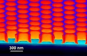
Image: Photonic crystal composed of a periodic array of holes etched in silicon slab. False-colored SEM image.
As described in today’s issue of the journal Nature, IBM scientists were able to slow light down to less than 1/300th of its usual speed by directing it down a carefully designed channel of perforated silicon called a “photonic crystal waveguide.” Further, the unique design of the device allows the light’s speed to be varied over a wide range simply by applying an electrical voltage to the waveguide.
Researchers have known for some years how to slow light to a crawl under laboratory conditions, but actively controlling the light speed on a silicon chip, using standard silicon with standard micro- and nanoelectronic fabrication technology, is a first. The device’s small size, use of standard semiconductor materials, and ability to more closely control this “slow light” could make the technology useful for building ultra-compact optical communications circuits that are practical for integration into computer systems.
“This work is an example of our continued commitment to push the limits of exploratory science,” said Dr. T.C. Chen, vice president of Science and Technology for IBM Research. “We are constantly exploring new technologies that might enhance our systems and storage products. We believe this brings real value to both our clients, who rely on these products to enhance their business, and to their customers, who ultimately benefit from the new and improved services they make possible.”
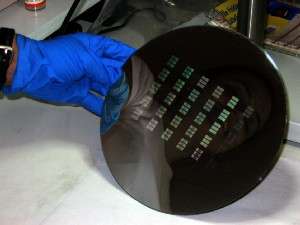
Image: SOI 200mm wafer processed on a standard CMOS fabrication line with numerous nanophotonic circuits
While chip performance has continued to increase, electronic systems don’t always reap the full benefits. Just as traffic congestion can hinder commerce by limiting the flow of products and materials within a busy city, the inability to more quickly move information around within electronic systems is one of the biggest bottlenecks in electronic design today. The work announced by IBM could help relieve such constraints.
Scientists have searched for practical ways to use light to speed communication between the components within a computer. But, to be practical, the components to support such an optical network will need to provide excellent control over the light signal, while also being very small and inexpensive to manufacture. The IBM work addresses several pieces of this puzzle.
The IBM team succeeded using a photonic crystal waveguide – a thin slab of silicon punctuated by regular arrays of holes that scatter light. The pattern and size of the holes gives the material a very high refractive index -- the higher the refractive index, the slower the light. Heating the waveguide locally with a small electrical current alters the refractive index, allowing the speed of light to be quickly tuned over a large range with very low applied electric power.
The active area of the IBM device is microscopically small, indicating the possibility of complex light-based circuits with footprints not much larger than semiconductor circuits. The manufacturing processes used to build the device are available in nearly any semiconductor factory. The capabilities demonstrated in today’s Nature article could be applied to create a variety of nanophotonic components such as optical delay lines, optical buffers, and even optical memory, all of which would be useful in building computer systems knitted together by powerful optical communications networks.
Animation: Active Control of Slow light on a chip (REFRESH the page to play again)
The report on this work, “Active control of slow light on a chip with photonic crystal waveguides” by Yurii A. Vlasov, Martin O’Boyle, Hendrik F. Hamann, and Sharee J. McNab of IBM’s T.J.Watson Research Center in Yorktown Heights, N.Y. is published in the November 3 issue of Nature. This work was partially supported by the Defense advanced Research Agency (DARPA) through the Defense Sciences Office program “Slowing, Storing and Processing Light”.
Source: IBM


