Bright nanotubes for telecom
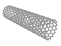
Carbon tubes only nanometers or billionths of a meter in diameter could serve as ultra-bright light sources for telecommunications, IBM scientists told UPI's Nano World. Conventional solid-state light sources such as light-emitting diodes, or LEDs, bring together positive and negative charges. When those charges neutralize each other, they emit pulses of light, or photons.
Materials suitable for such optical applications often are not ideal for electronic applications, said electronics researcher and materials scientist Jia Chen at IBM's research division in Yorktown Heights, N.Y. On the other hand, carbon nanotubes are superb electronics materials, and their physical qualities suggested they are potentially excellent optical materials as well, she explained.
"Nowadays information mostly travels as photons in optical fibers deep beneath the ocean," Chen said. The hope is that carbon nanotubes could serve as construction blocks to help integrate optical and electronic components onto the same chip, greatly enhancing miniaturization in telecommunications devices.
Moreover, as semiconductor-based electronics become ever smaller, "the metal wirings currently used to connect the different components on a single chip will suffer increasingly from problems such as lack of speed and unacceptable levels of power dissipation, eventually limiting the chip performance. These on-chip emitters can provide an attractive alternative as optical connections that potentially eliminate these problems," Chen said.
Scientists had endeavored to create light sources from carbon nanotubes before, but earlier attempts led to very inefficient devices, Chen said. Prior designs introduced positive and negative charges simultaneously from opposite ends of the nanotubes, but injecting the same amounts of positive and negative charges at the same time "is not an easy task," she explained. "The chances that they meet each other and emit photons are quite low."
Chen and her colleagues designed light sources that generate 100,000 times more photons per unit area per second than conventional LEDs do. Moreover, they are 1,000 times more efficient than prior carbon nanotube devices. This improved efficiency stems from a design that no longer injects positive and negative charges from opposite ends of nanotubes. Instead, the researchers suspend the nanotubes in surface-oxidized silicon wafers. This leads to high electric fields near the junction between the nanotubes and the wafers. In turn, electrons injected into the nanotubes pick up energy, creating negative-positive charge combinations that recombine to form light. Their findings appear in the Nov. 18 issue of the journal Science.
The nanotubes emit light "with a wavelength of one to two micrometers, which is particularly valuable because it is the wavelength widely used in optical communications," said Phaedon Avouris, manager of nanometer-scale science technology at IBM's research division. Physical chemist Bruce Weisman at Rice University in Houston called the IBM findings "an important advance" that could accelerate applications for carbon nanotubes.
Copyright 2005 by United Press International


