Fujitsu Pioneers Use of Carbon Nanotubes for Heatsinks for Semiconductors
Fujitsu today announced that they have succeeded in the world's first development of carbon nanotube-based heatsinks for semiconductor chips. The use of carbon nanotubes as heatsinks for high-frequency high power amplifiers successfully achieves heat dissipation and high amplification simultaneously.
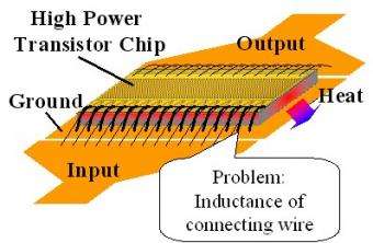
Figure 1: Face-up mounted high power amplifier
The new technology represents a major step forward in developing practical applications that take advantage of the superior thermal conductivity of carbon nanotubes. It also enables the realization of high-performance amplifiers with high frequency and high power for next-generation mobile communication systems.
Details of the technology will be presented at the IEEE International Electron Devices Meeting (IEDM) to be held in Washington, D.C. from December 5. This research is part of the Advanced Nanocarbon Application Project consigned to the Japan Fine Ceramics Center, by Japan's New Energy and Industrial Technology Development Organization (NEDO).

The volume of information transmitted in our information age continues to grow, and in wireless communications there is an increasing demand for higher power and higher frequencies in amplifiers used in mobile phone base stations. Because high power transistors, the output source for high-performance amplifiers, generate high levels of heat, heat dissipation is extremely important. Conventionally, heat was dissipated through the use of what is known as the "face-up structure" (Figure 1), in which a high power transistor chip would be connected directly dice-bonded to the package and the heat would escape through the chip.
At higher frequencies, amplifiers using the face-up structure suffer from reduced amplification. The cause is inductance from the metal wire, through which the electrical current flows from the electrode of the transistor chip to the electrode of the package. One solution is to flip over the transistor chip and connect the chip electrode and the package electrode with short metallic bumps made from gold or other metals, in what is known as a "flip-chip structure"(Figure 2). However, for use in high power amplifiers, conventional metallic bumps have proven inadequate in dissipating the high levels of heat generated by high-power transistors. For these reasons, it has been difficult to develop high-performance amplifiers that can satisfy both high-amplification and heat dissipation at high frequencies.
Fujitsu's new technology enables the simultaneous achievement of high amplification and heat dissipation, in high-frequency, high power amplifiers. Fujitsu has succeeded in the world's first application of carbon nanotubes, which have excellent thermal conductivity, for the bumps in a flip-chip structure (Figures 2 and 3).

Key features of the technology:
1. Technology to grow carbon nanotubes This is a technology that uses an iron catalyst coating to grow carbon nanotubes to a vertical length of at least 15 micrometers on the wafer substrate. Usually, bumps for flip-chips are required to have a length of at least 10 micrometers.
2. Technology to connect the carbon nanotube bump to the flip-chip Taking advantage of the process miniaturization features of carbon nanotubes, by forming a miniature carbon nanotube bump patterned to match a high power transistor's miniature electrode pattern with a width no greater than 10 micrometers, Fujitsu succeeded in connecting the carbon nanotube bump to the flip-chip.
With the technology, Fujitsu was able to connect carbon nanotube bumps to the miniature electrode of a high power transistor. Carbon nanotubes have thermal conductivity of 1400W/(m-K) - a level much higher than that of metal, and because it is possible to connect carbon nanotube-based bumps very near to the heat-generating miniature electrodes, Fujitsu successfully achieved the high amplification of flip-chips with heat dissipation levels equivalent to face-up structures. Compared to conventional face-up structures, ground inductance is reduced by more than half, thereby enabling an increase in amplification of at least 2 decibels at high frequencies of 5 gigahertz or greater.
Fujitsu intends to continue to refine the site density of carbon nanotubes in bumps to enable further improvements in heat dissipation, paving the way for development of high-frequency, high power flip-chip amplifiers using carbon nanotube bumps. Fujitsu targets deployment of this new technology in base stations for next-generation mobile communication systems in approximately three years.
Source: Fujitsu


