Research removes major obstacle from mass production of tiny circuits
As they eliminate tiny air bubbles that form when liquid droplets are molded into intricate circuits, a Princeton-led team is dissolving a sizable obstacle to the mass production of smaller, cheaper microchips.

Led by Stephen Chou, the Joseph C. Elgin Professor of Engineering at Princeton, the team worked to troubleshoot one form of nanoimprint lithography, a revolutionary method invented by Chou in the 1990s.
Nanoimprint uses a nanometer-scale mold to pattern computer chips and other nanostructures, and is in marked contrast to conventional methods that use beams of light, electrons or ions to carve designs onto devices.
This technique allows for the creation of circuits and devices with features that are not much longer than a billionth of a meter, or nanometer -- more than 10 times smaller than is possible in today's mass-produced chips, yet more than 10 times cheaper. Because of its unique capabilities and reasonable cost, nanoimprinting is a key solution to the future manufacturing of computer chips and a broad range of nanodevices for use in optics, magnetic data storage and biotechnology, among other disciplines.
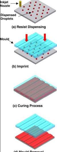
In dispensing-based nanoimprinting, liquid droplets on the surface of a silicon wafer are pressed into a pattern, which quickly hardens to form the desired circuitry. This technique is more attractive to manufacturers than some other forms of nanoimprinting because it does not need to be done in an expensive vacuum chamber. However, the widespread use of the technique has been hindered by the formation of gas bubbles that distort the intended pattern.
"This is an important step because to benefit from the technology of nanoimprinting you need to be able to use it in mass manufacturing at low cost," Chou said. The team's findings are reported today (Jan. 17, 2007) in the journal Nanotechnology.
In a series of experimental and theoretical studies, Chou and his colleagues studied the factors that cause air bubbles to form and explored ways to eliminate the sub-millimeter-sized scourges. By increasing the imprinting pressure or using liquids that have higher air solubility, they were able to dramatically increase the likelihood that the bubbles would dissolve in the liquid before it hardened.
Citation: Liang, Tan, Fu and Chou. Air bubble formation and dissolution in dispensing nanoimprint lithography. Jan. 17, 2007. Nanotechnology. doi:10.1088/0957-4484/18/2/025303.
Source: Princeton University


