AMO Manufactures First Graphene Transistors

February 8, 2007 AMO Manufactures First Graphene Transistors

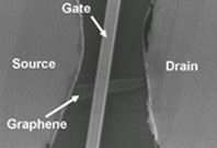
In the scope of his innovative project ALEGRA the AMO nanoelectronics group of Dr. Max Lemme was able to manufacture top-gated transistor-like field-effect devices from monolayer graphene.

Compared to conventional silicon and SOI MOSFETs the researchers realized a significant enhancement of electron and hole mobility.

Moore’s law, which has dictated ambitious innovation cycles to the semiconductor industry over the last decades, may finally be running out of steam. In the future, innovations for silicon technology may only be realized by integrating new functionalities or novel materials.

Carbon is one of the most probable candidates: impressive potential for nanoelectronics applications has been demonstrated with carbon nanotubes – and graphene!

A conventional CMOS-compatible process has been applied to fabricate a graphene field-effect device – a transistor made from a monolayer of carbon. The observed mobility in the devices exceeds the universal mobility in silicon MOSFETs. Furthermore, a second transistor gate was placed on top of the graphene film for the first time. AMO’s results confirm the high potential of graphene for future nanoelectronic devices.

First experimental details will be published in IEEE Electron Device Letters in April 2007.

Citation: M.C. Lemme, T.J. Echtermeyer, M. Baus, H. Kurz, “A Graphene Field Effect Device”, IEEE Electron Device Letters, Vol. 28, No. 4, April 2007.

Source: AMO


print this article email this article download pdf blog this article bookmark this article     Stumble it Digg this share on Facebook retweet share on Reddit add to delicious
Rate this story - 4.1 /5 (18 votes)


February 8, 2007 all stories

Comments: 0

4.1 /5 (18 votes)
  • Stumble this up

  • Digg this

  • share this

  • hide
  • Related Stories


  • hide
  • Relevant PhysicsForums posts

  • Voltage drop in diode
    created 19 hours ago
  • ZENER BREAKDOWN has caused me a breakdown
    created Nov 20, 2009
  • Transistor AMPLifier HelP !!!!
    created Nov 20, 2009
  • A loophole in Kubo formula
    created Nov 20, 2009
  • More from Physics Forums - Atomic, Solid State, Comp. Physics

Other News

Using superconducting probes to get a picture of what it's like inside CNTs

Nanotechnology / Nanophysics

created Nov 20, 2009 | popularity 4.9 / 5 (7) | comments 0

(PhysOrg.com) -- "Carbon nanotubes are exciting for fundamental physics, and for potential technological applications," Nadya Mason tells PhysOrg.com. "However, we are generally limited in the way that we can study them. ...


Nanoparticles used in common household items caused genetic damage in mice

Nanotechnology / Bio & Medicine

created Nov 16, 2009 | popularity 4.7 / 5 (22) | comments 11

Titanium dioxide (TiO2) nanoparticles, found in everything from cosmetics to sunscreen to paint to vitamins, caused systemic genetic damage in mice, according to a comprehensive study conducted by researchers at UCLA's Jonsson ...


Nanotube defects equal better energy and storage systems

Nanotube defects equal better energy and storage systems

Nanotechnology / Nanomaterials

created Nov 19, 2009 | popularity 4.4 / 5 (9) | comments 2

(PhysOrg.com) -- Most people would like to be able to charge their cell phones and other personal electronics quickly and not too often. A recent discovery made by UC San Diego engineers could lead to carbon ...


When It Comes to Drug Delivery, Size Matters

Nanotechnology / Bio & Medicine

created Nov 20, 2009 | popularity 5 / 5 (1) | comments 0

(PhysOrg.com) -- One of the great promises of nanotechnologies lies in its ability to create drug-containing nanoparticles decorated with targeting molecules that recognize and bind to cancer cells, providing drug delivery ...


Scientists synthesize graphene-like material: Polymer with honeycomb structure

Scientists synthesize graphene-like material: Polymer with honeycomb structure

Nanotechnology / Nanomaterials

created Nov 19, 2009 | popularity 4.5 / 5 (6) | comments 1

Two-dimensional carbon layers, so-called graphenes, are regarded as a possible substitute for silicon in the semiconductor industry. The electronic properties of these layers can be varied by "building in" ...