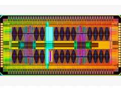
IBM Reveals Breakthrough eDRAM Memory Technology

In papers presented at the International Solid State Circuits Conference, IBM revealed a first-of-its-kind, on-chip memory technology that features the fastest access times ever recorded in eDRAM (Embedded Dynamic Random Access Memory). IBM's new microchip technology will more than triple the amount of memory stored on chips and double the performance of computer processors. It will be available in 2008.
This new technology, designed using IBM’s Silicon-on-Insulator (SOI) for high-performance at low power, vastly improves microprocessor performance in multi-core designs and speeds the movement of graphics in gaming, networking, and other image intensive, multi-media applications.
The technology is expected to be a key feature of IBM’s 45nm microprocessor roadmap and will become available beginning in 2008.
IBM’s new eDRAM technology, designed in stress-enabled 65nm SOI using deep trench, dramatically improves on-processor memory performance in about one-third the space with one-fifth the standby power of conventional SRAM (static random access memory).
“With this breakthrough solution to the processor/memory gap, IBM is effectively doubling microprocessor performance beyond what classical scaling alone can achieve,” said Dr. Subramanian Iyer, Distinguished Engineer and director of 45 nm technology development at IBM. “As semiconductor components have reached the atomic scale, design innovation at the chip-level has replaced materials science as a key factor in continuing Moore’s Law. Today’s announcement further demonstrates IBM’s leadership in this critical area of microprocessor design innovation.”
IBM innovations in microelectronics and the company's groundbreaking system-on-a-chip designs have transformed the world of semiconductors. IBM breakthroughs include High-k, which enhances the transistor’s function while allowing it to be shrunk beyond today's limits, dual-core and multi-core microprocessors, copper on-chip wiring, silicon-on-insulator and silicon germanium transistors, strained silicon, and eFUSE, a technology that enables computer chips to automatically respond to changing conditions. The White House has awarded IBM the National Medal of Technology, the nation's highest technical honor, for 40 years of innovation in semiconductors.
IBM chips are the heart of the company's server and storage systems, the world's fastest supercomputers and many of the best-known and widely used communications and consumer electronics brands.
New eDRAM Specifications:
Among the specifications of IBM’s high-performance eDRAM technology:
Cell size: 0.126 mm2
Power supply: 1 V
Availability: 98.7%
Tile: 1K RowX16 Col X146 (2Mb)
AC power: 76 mW
Standby keep alive Power: 42 mW
Random cycle time: 2ns
Latency: 1.5ns
Source: IBM Microelectronics


