Samsung Begins World's First 60nm-DRAM Mass Production
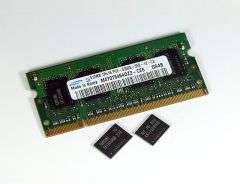
Samsung Electronics announced today that it has begun mass producing the industry’s first 1Gigabit (Gb) DDR2 DRAM (dynamic random access memory) using 60 nanometer (nm)–class process technology.
Use of the new process technology is a significant milestone in that it increases production efficiency by 40 percent over the 80nm process technology deployed in DRAM fabrication since early 2006, and offers twice the productivity of 90nm general process technology.
Ample market availability of 1Gb DRAM will further increase the demand for large density DRAMs, especially as the new premium Vista operating system imposes a DRAM requirement of at least 1Gigabyte (GB). Samsung’s extensive line up of 60nm 1Gb DRAM-based modules includes 512MB, 1GB, and 2GB densities supporting either 667Mbps or 800Mbps speeds with customer validation.
Samsung anticipates such a high degree of receptivity to the 60nm process that it should drive greater demand for 1Gb DRAM chips in the near future over today’s mainstream density of 512Mb.
Samsung’s continuous technology migration below 90nm has relied heavily on the company’s extensive use of three-dimensional (3D) transistor technologies to build increasingly smaller chips, a fundamentally unique approach toward finer circuit designs and higher yields. One of the key technologies involved in the development of Samsung’s 3D transistor is a recess channel array transistor (RCAT) that actually builds the DRAM cell three-dimensionally to minimize its size while increasing its density.
Samsung’s proprietary RCAT technology was first introduced at the 2003 VLSI symposia. This new 3D transistor technology doubles the refresh cycle, which is critical for enabling efficient fabrication on a nanometer-scale. Samsung has been utilizing RCAT for DRAM fabrication from 90nm. This key 3D technology is expected to enable DRAM fabrication to 50nm and lower.
In addition to its 60nm process technology innovation, Samsung’s use of metal-insulator metal (MIM) for its capacitors provides enhanced data storage in sub-70nm designs.
Furthermore, the use of a recently-announced selective epitaxial growth (SEG) technology provides for a broader electron channel, and optimizes the speed of each chip’s electrons to reduce power consumption and enable higher performance.
The 60nm 1Gb DDR2 DRAM, which was first developed by Samsung in 2005, is the latest in a long line of Samsung industry “firsts” in nano-scale DRAM advancements. This record of DRAM innovation stretches from the introduction of 150nm DRAM technology in 2000, to a yet-to-be-deployed 50nm process technology developed in October of last year.
The 60nm process is expected to become the mainstream circuit technology for DRAM in 2008. In the first year of market availability alone, 60nm DRAM revenues are expected to reach US $2.3billion worldwide and further increase to US $32 billion by 2009.
Source: Samsung


