Duke Chemist's Lab Steady Source of 'Nanotube' Advances
"Nanotubes" grown in the busy laboratory of associate chemistry professor Jie Liu were crucial to IBM scientists' recent announcements of a new source of light emissions. Liu's lab is also working with a California firm to pioneer use of these infinitesimally-thin carbon tubes in place of copper contacts for computer chips.
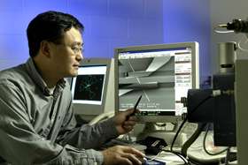
Image: Jie Liu works to find new applications for carbon nanotubes
These are just the latest examples of Liu's group's work with nanotubes, sometimes nicknamed "buckytubes" because of their architectural similarities to soccer-ball shaped molecules of carbon called buckminsterfullerines or "buckyballs.
These single-atom-thick cylinders of carbon are attracting scientific and industrial attention for their unusual and useful properties. They are called nanotubes because their diameters are measured in the billionths of a meter, the prefix "nano" meaning "billionths."
Even though they are ultra thin and ultra light, nanotubes form exceptionally strong, stiff and tough fibers that conduct heat and electricity exceptionally well and can even be made to self-assemble. Nanotubes of sufficient purity also have unusual electrical properties, behaving either like semiconductors or like metals depending on their specific molecular architectures.
All these properties make them strong candidates to become the basis of futuristic molecular-scale nanoelectronic circuitry and nanostructures, said Liu, who came to Duke from the Rice University laboratory of a buckyball and buckytube pioneer -- the late Nobel laureate Richard Smalley.
In an April, 2003 online edition of the Journal of the American Chemical Society, Liu and members of his group announced a method to grow exceptionally stretched-out nanotubes that -- while they measure the usual few nanometers in width -- can extend well beyond the nano scale for more than 2 millimeters in length.
Liu's lab has since begun supplying long nanotubes to IBM, where company scientists found the tiny structures can serve as microscopic light emitters when made components of experimental transistors.
In the Nov. 18 issue of the journal Science, in a paper that included Liu and his graduate student Qiang Fu as coauthors, an IBM team led by Phaedon Avouris reported achieving unprecidentedly bright infrared light outputs using a modified nanotube transistor.
The modification involved growing the nanotubes over a tiny trench excavated in the chip's surface, the Science authors reported. The introduction of the trench altered electron properties in a way that caused light to be emitted at a point of high electrical fields where the nanotube and one trench edge intersected.
"The extraordinary current-carrying capability of a carbon nanotube and its ultra-small size lead to an ultra-bright light source," the authors wrote in the paper.
"Our contribution to this project was that we are the group that can grow nanotubes extending all the way across the trenches," Liu said. "Other methods wouldn't be able to do that."
While the nanotubes used for the IBM work were relatively short, ranging in the hundredths of a millimeter, Liu said the longest nanotubes his group is growing measure in the centimeters.
In another project, Arrowhead Research Corp., a Pasadena, Calif. nanotechnology firm, also announced in November that it would work with Liu's laboratory to develop nanotube-based interconnects that would replace copper connectors within computer chip circuitry that continues to miniaturize.
"As consumer demand grows for smaller and faster chips, copper interconnects become more and more difficult and costly to fabricate," the company announcement said. "We believe the Duke team has a unique solution to this problem."
Liu said copper connectors can degrade and fail from severe heating when required to carry considerable current loads over increasingly small circuit dimensions. "Substituting carbon nanotubes, in theory, can really solve this problem," he said.
The challenge for his group will be "to develop a method to put nanotubes where you want them to be in a manner that can be scaled up to full wafer scale," Liu said. "Our main research direction will be developing such methods."
Source: Duke University


